Design a Sr-latch With Enable Using a D-latch and Gates
Flip-Flops and Registers
Latches
A latch is a temporary storage device that has two stable states (bistable). It is a basic form of memory. The S-R (Set-Reset) latch is the most basic type. It can be constructed from NOR gates or NAND gates. With NOR gates, the latch responds to active-HIGH inputs; with NAND gates, it responds to active-LOW inputs.
S-R Flip-Flop
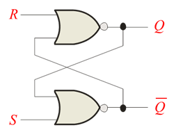
- A S-R flip-flop can also be made using cross-coupled NAND gates.
- The cross-coupled NAND flip-flop has low active set and reset inputs. These can be made high active by using inverters.
- A flip-flop is "latched" when the Q output hold the last input condition.
- A flip-flop is said to be transparent when the Q output responds immediately to a change on the input.
- A register is a group of flip-flops used to store a binary word. One flip-flop is needed for each bit in the data word.
- AND gates can be used to "strobe" or enable data gated into a register.
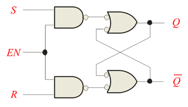
Gated S-R Flip-Flop
- A gate input is added to the S-R flip-flop to make the flip-flop synchronous.
- In order for the set and reset inputs to change the flip-flop, the gate input must be active (high).
- When the gate input is low, the flip-flop remains in the hold condition.
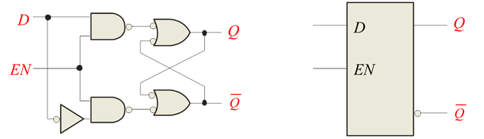
Gated D Flip-Flop
- The D (data) flip-flop has a single input that is used to set and to reset the flip-flop.
- When the gate is high, the Q output will follow the D input.
- When the gate is low, the flip-flop is latched.
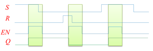
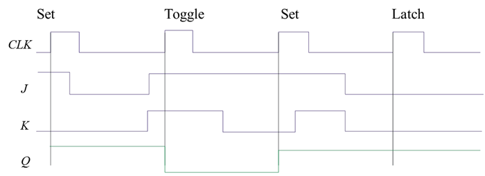
A simple rule for the D latch is:
Q follows D when Enabled.
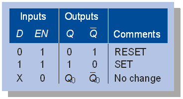
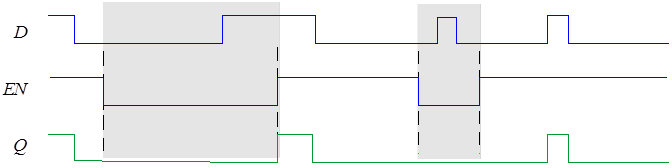
Notice that the Enable is not active during the grey areas, so the output is latched.
The Integrated-Circuit D Latch (7475)
- The 7475 contains 4 transparent D latches with a common enable (gate) on latches 0 and 1 and another common enable on latches 2 and 3.
- When Q follows D (latch enabled) the latch is said to be transparent.
The Integrated-Circuit D Flip-Flop (7474)
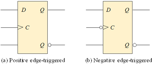
- The 7474 is an edge-triggered device. The Q output will change only on the edge of the input trigger pulse.
- The small triangle on the clock (Cp) input of the symbol indicates that the device is positive edge-triggered.
- The D and the clock inputs are synchronous inputs.
- The set (SD) and reset (RD) inputs are asynchronous. They operate independent of D and Cp.
- The bubbles on the set and reset inputs indicate that they are low active.
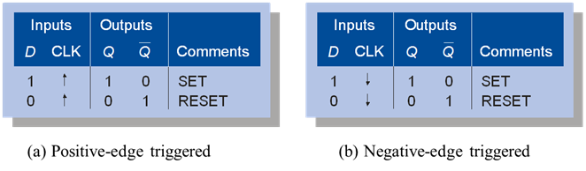
The truth table for a positive-edge triggered D flip-flop shows an up arrow to remind you that it is sensitive to its D input only on the rising edge of the clock; otherwise it is latched. The truth table for a negative-edge triggered D flip-flop is identical except for the direction of the arrow.
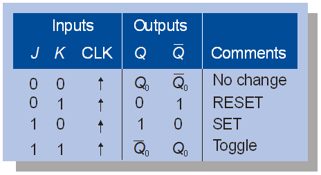
Master—Slave J-K Flip-Flop
- The J-K flip-flop has a toggle mode of operation when both J and K inputs are high. Toggle means that the Q output will change states on each active clock edge.
- J, K and Cp are all synchronous inputs.
- The master—slave flip-flop is constructed with two latches. The master latch is loaded with the condition of the J-K inputs while the clock is high. When the clock goes low, the slave takes on the state of the master and the master is latched.
- The master—slave is a level-triggered device.
- The master—slave can interpret unwanted signals on the J-K inputs.
- These are not used as often in modern electronics
Edge-Triggered J-K Flip-Flop
- The edge-triggered J-K will only accept the J and K inputs during the active edge of the clock.
- The small triangle on the clock input indicates that the device is edge-triggered.
- A bubble on the clock input indicates that the device responds to the negative edge. No bubble would indicate a positive edge-triggered device.
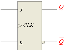
Integrated-Circuit J-K Flip-Flop (7476, 74LS76)
- The 7476 is a master—slave J-K and the 74LS76 is a negative edge-triggered J-K flip-flop.
- Both chips have the same pin configuration.
- Both chips have synchronous inputs of J, K and Cp.
- Both chips have asynchronous inputs.
- The J-K flip-flop can be made into a D flip-flop by bringing the data input into the J and the inverse of the data input into the K input.
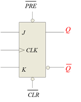
- Synchronous inputs are transferred in the triggering edge of the clock (for example the D or J-K inputs). Most flip-flops have other inputs that are asynchronous, meaning they affect the output independent of the clock.
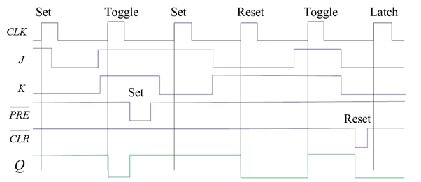
- Two such inputs are normally labeled preset (PRE) and clear (CLR). These inputs are usually active LOW. A J-K flip flop with active LOW preset and CLR is shown.
Flip-flop Characteristic
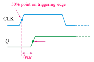
Propagation delay time is specified for the rising and falling outputs. It is measured between the 50% level of the clock to the 50% level of the output transition.
The typical propagation delay time for the 74AHC family (CMOS) is 4 ns. Even faster logic is available for specialized applications.
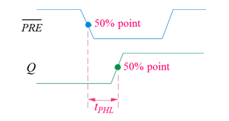
Another propagation delay time specification is the time required for an asynchronous input to cause a change in the output. Again it is measured from the 50% levels. The 74AHC family has specified delay times under 5 ns.
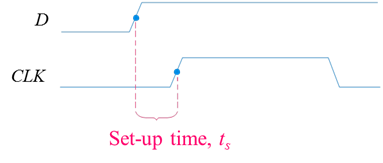
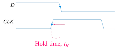
Set-up time and hold time are times required before and after the clock transition that data must be present to be reliably clocked into the flip-flop.
Setup time is the minimum time for the data to be present before the clock.
Hold time is the minimum time for the data to remain after the clock.
Flip-flop Applications
Principal flip-flop applications are for temporary data storage, as frequency dividers, and in counters.
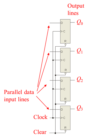
Typically, for data storage applications, a group of flip-flops are connected to parallel data lines and clocked together. Data is stored until the next clock pulse.
For frequency division, it is simple to use a flip-flop in the toggle mode or to chain a series of toggle flip flops to continue to divide by two.
One flip-flop will divide f in by 2, two flip-flops will divide f in by 4 (and so on). A side benefit of frequency division is that the output has an exact 50% duty cycle.

Design a Sr-latch With Enable Using a D-latch and Gates
Source: https://grace.bluegrass.kctcs.edu/~kdunn0001/files/Flip_Flops/Flip_Flops_print.html
0 Response to "Design a Sr-latch With Enable Using a D-latch and Gates"
Post a Comment